TSMC Q3 revenue jumps 30% on AI-fueled chip demand, beats forecasts
TSMC, the world’s largest contract chipmaker, posted a 30% year-on-year surge in third-quarter revenue, driven by the global boom in artificial intelligence demand. The company’s performance outpaced analyst expectations, reaffirming its dominance in the semiconductor supply chain that powers AI leaders like Nvidia and Apple.
Revenue for the July–September period reached T$989.92 billion ($32.47 billion), surpassing the T$973.26 billion consensus estimate from 22 analysts compiled by LSEG SmartEstimate. The figure landed in the midpoint of TSMC’s July guidance of $31.8 billion–$33 billion, according to its previous earnings call.
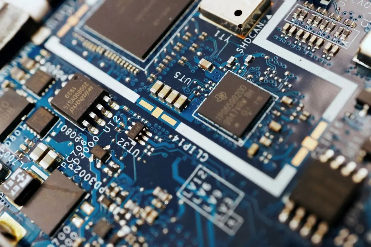
The strong result underscores how AI-related chip demand is offsetting slower sales of consumer electronics such as smartphones and tablets. TSMC’s cutting-edge chips are essential for powering advanced AI systems and high-performance computing, both of which have fueled a new growth cycle for the company.
TSMC’s Taipei-listed shares have climbed 34% year-to-date, outpacing the broader Taiwan index’s 18.5% gain. Analysts expect the company’s October 16 earnings report to include a revised full-year outlook, likely reflecting continued AI-driven momentum.
The upbeat results mirror a wider surge across Taiwan’s tech sector: Foxconn, Nvidia’s largest server manufacturer, also posted record-high third-quarter revenue, signaling sustained strength in the AI hardware supply chain.