Advancing Nanoscale Imaging with Laser Technology
Scientists have developed a cutting-edge laser imaging technique to analyze nanoscale heat and charge transport in ultrawide-bandgap semiconductors like diamond. Using a deep-ultraviolet (DUV) laser, this method achieves an impressive spatial resolution of 287 nanometres, surpassing the limitations of traditional visible-light imaging. By enhancing the study of diamond’s transport properties, this breakthrough paves the way for improvements in high-performance power electronics and communication systems.
Revolutionary DUV Microscopy for Semiconductor Research
A recent study in Physical Review Applied highlights the development of a DUV microscope capable of producing interference patterns on material surfaces, enabling detailed heat mapping at the nanoscale. The research, led by JILA scientists Margaret Murnane and Henry Kapteyn, involved collaborations with graduate students and industrial partners from 3M. Unlike visible-light methods, which struggle with ultrawide-bandgap materials, this new approach overcomes fundamental energy gap challenges, offering unprecedented imaging precision.
Technical Innovation and System Optimization
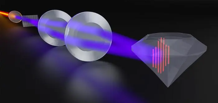
The DUV system was constructed by converting 800-nanometre laser pulses into shorter wavelengths using nonlinear crystals, generating high-energy light essential for nanoscale analysis. This innovation allows researchers to create transient gratings on semiconductor surfaces, providing a deeper understanding of their thermal and electronic properties. Years of development and meticulous testing were required to optimize the system, with researchers fine-tuning the laser alignment to ensure precise nanoscale pattern formation.
Future Impact on Semiconductor and Electronic Technologies
By refining imaging capabilities at the nanoscale, this technique has the potential to revolutionize semiconductor research and device engineering. Enhanced understanding of heat and charge transport in diamond and other ultrawide-bandgap materials could lead to more efficient, durable power electronics and faster communication networks. As the demand for high-performance electronics grows, the insights provided by DUV microscopy will be invaluable in driving future technological advancements.